One controversy to mar the launch of Siri AI was the news that it will not as yet be available within EU countries . The EU told Apple that it would have to allow third-party AI providers to offer similar functionality on iPhones, and the company has responded by withholding an EU launch for now. We’re now learning that Meta’s WhatsApp is being faced with a similar demand …
A number of people have been complaining that the new Siri demos during the keynote videos were a little on the slow side. There were notable lags of several seconds between Siri requests and the task being carried out. But while the ideal we’re aiming for is for AI tasks to be carried out as quickly as possible, what we saw is kind of good news …
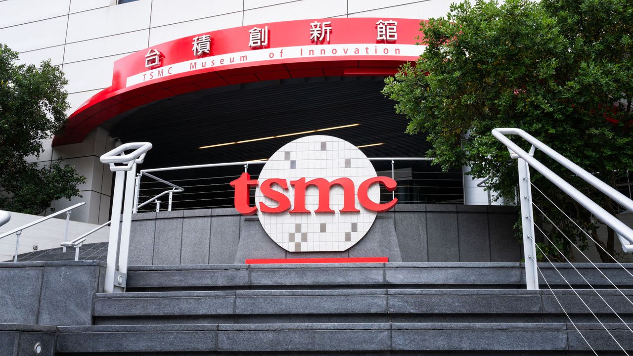
TSMC is executing the largest manufacturing expansion in semiconductor industry history that combines simultaneous multi-fab N2 ramps, AI-driven manufacturing optimizations, and massive CoWoS/SoIC packaging capacity expansion to meet increasing demand for AI accelerators.
Save $800 on this customizable RTX 5070 Ti HP Omen Max 16 gaming laptop with 16GB DDR5, 1TB SSD, and a 16-inch display.
MIT's 3D-printed triaxial electrospray nozzles could revolutionize drug and self-healing material manufacturing. By using a relatively inexpensive resin printing approach, the new nozzle fabrication technique removes the need for a semiconductor-class cleanroom facility.
Despite making the jump to video-on-demand on digital platforms last month, The Super Mario Galaxy Movie is still holding its theatrical position in cinemas in some locations. Now, it's finally pushed its global box office haul past the $1bn mark. Read more
Researchers at EPFL have developed a chip-scale ultrafast laser that performs on par with traditional tabletop femtosecond lasers. The innovation could make advanced laser technologies far smaller, cheaper, and more accessible for applications ranging from medical diagnostics to atomic clocks.
As traditional chip miniaturization slows, researchers have found a way to pack more computing power into the same space by stacking silicon circuits in multiple layers. The new process uses ultra-thin silicon membranes and low-temperature manufacturing techniques to overcome a major obstacle that has long blocked the production of true 3D chips.
I have been an application-specific IC (ASIC) designer for almost three decades. Over that time, I’ve moved through the full academic trajectory, from graduate student to full professor; later, I transitioned to industry after an unsuccessful stint at entrepreneurship. When I made the switch to the private sector in 2019, I began focusing on a critically important aspect of the electronic…